
What is MicroLED?
MicroLED is a kind of light emitting diode (LED), the size is usually less than 100 microns (m), the common size is less than 50 m, and some are even only 3-15 m. In terms of proportions, the size of a microLED is about 1/100 the size of a traditional LED, and about 1/10 the width of a human hair. In a microLED display, each pixel (each diode) is individually addressed and driven to emit light without a backlight (similar to OLED displays). They are made of inorganic materials and provide a long service life ( Similar to LED).
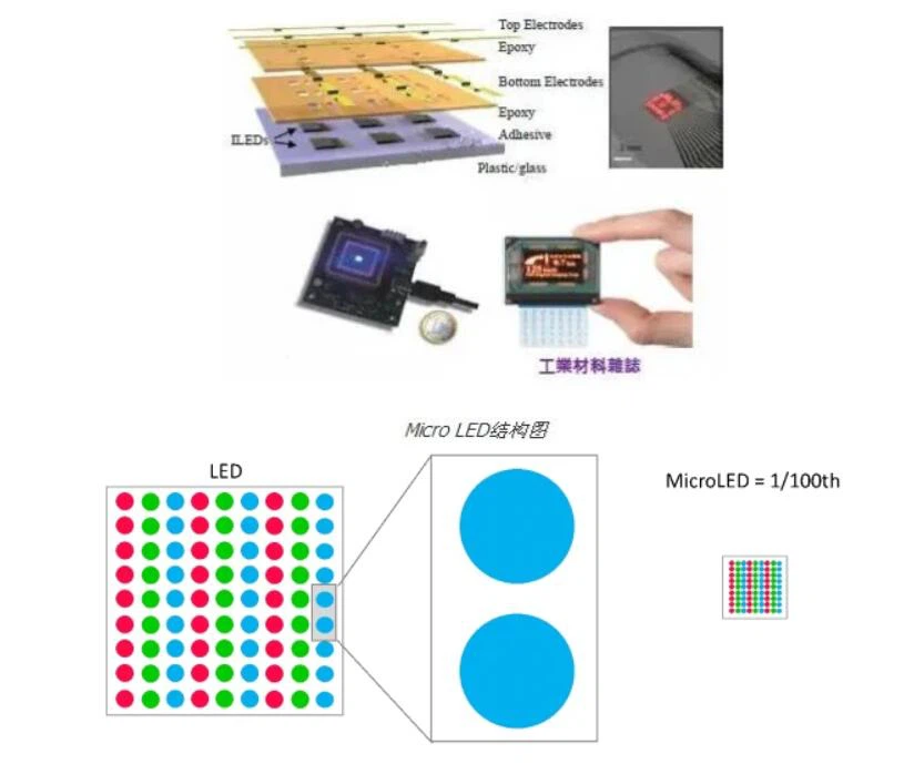
MicroLED has a maximum number of pixels per inch (PPI) of 5,000 and a brightness of 105 nits, while OLED has a maximum number of pixels per inch (PPI) of 3500 and a brightness of ≤2 x 10³ nits. 1 And like OLED, MicroLED advantage
High brightness, low power consumption, ultra-high resolution and color saturation. The biggest advantage of MicrolED comes from its biggest feature, the micron-level pitch, each pixel (pixel) can be addressed and controlled and single-point driven to emit light. Compared with other LEDs, MicroLED currently ranks high in terms of luminous efficiency, and the room is still being greatly improved; in terms of luminous energy density, MicroLED ranks high, and there is still room for improvement. ——The former is conducive to the energy saving of display devices, and its power consumption is about 10% of LCD and 50% of OLED; the latter can save the limited surface area of display devices and deploy more sensors. The current theoretical result is Compared with OLEDD, MICROLED achieves the same display brightness, and only needs about 10% of the coating area of the latter. Compared with the OLED, which is also a self-luminous display, the brightness is 30 times higher, and the resolution can reach 1500PPI (pixel density), which is equivalent to 5 times that of the OLED panel used by AppleWatch to reach 300PPI.
long life. Since Micro-LED uses inorganic materials and has a simple structure with almost no light consumption, its service life is very long. This is incomparable to OLED. As an organic material and organic substance, OLED has its inherent shortcomings—that is, lifespan and stability, which are difficult to compare with QLED and MICROLED of inorganic materials.
Can adapt to various sizes. The microLED can be deposited on different substrates such as glass, plastic and metal to achieve flexible, bendable and foldable displays.
There is a lot of room for cost reduction. At present, the micro-projection technology is mainly based on three technologies: Digital Light Processing (DLP), reflective silicon liquid crystal display (Liquid Crystalon Silicon, LCoS), and MEMS Scanning (MEMS Scanning), but these three technologies must use an external light source. It is not easy to further reduce the volume of the module, and the cost is also higher. In contrast, the self-luminous MicroLED microdisplay does not require an external light source, and the optical system is simpler, so it has advantages in miniaturization and cost reduction of the module volume
Micro LED application market
In the short term, the Micro-LED market is concentrated in ultra-small displays. In the medium and long term, Micro-LED has a wide range of applications, spanning wearable devices, large indoor display screens, head-mounted displays (HUD), and head-up displays. (HUD), car tail lights, wireless optical communication Li-Fi, AR/VR, projectors and other fields.
Micro LED technology principle
The display principle of MicroLEDDisplay is to thin, miniaturize, and array the LED structure design, and its size is only about 1~10μm; then, the MicroLED is transferred to the circuit substrate in batches, and the substrate can be either rigid or flexible. On a transparent and opaque substrate; the protective layer and upper electrode are then completed by a physical deposition process, and the upper substrate can be packaged to complete a simple structure of MicroLED display.
To make a display, the chip surface must be made into an array structure like an LED display, and each dot pixel must be addressable and controllable and individually driven to light up. If driven by a complementary metal oxide semiconductor circuit, it is an active addressing drive architecture, and the packaging technology can be used between the MicroLED array chip and the CMOS.
After the pasting is completed, the MicroLED can improve the brightness and contrast by integrating the micro lens array. The MicroLED array connects the positive and negative electrodes of each MicroLED through vertically staggered positive and negative grid electrodes. The electrode lines are sequentially energized, and the MicroLED is illuminated by scanning to display images.
As an emerging link in the industry chain, Micro LED has a highly difficult process that is rarely used in other electronics industries—massive micro-transfers (also called massive transfers). Mass transfer is regarded as the core factor affecting yield and capacity release, and it is also the area where major manufacturers focus on tackling tough problems. At present, there are also different directions in the technical route, namely laser transfer, self-assembly technology, and transfer technology.
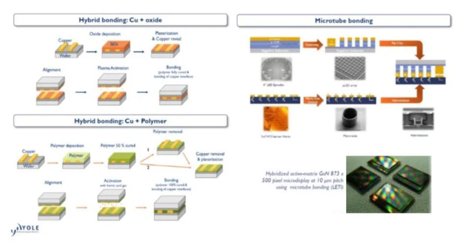
What kind of technology is "mass transfer"? Simply put, on a TFT circuit substrate the size of a fingernail, in accordance with the necessary specifications of optics and electricity, evenly solder three to five hundred, or even more, red, green and blue three primary color LED tiny dies, and what is the allowable process failure rate? One hundred thousandth. ——Only products with such a craftsmanship can be truly applied to products such as AppleWatch3.
Regarding the process of MicroLED, many people believe that experience can be learned from traditional LED screens. However, there is a huge difference between MicroLED and traditional LED display products. Compared with traditional LED display screens, the main differences of MicroLED are: 1. The degree of precision is increased by dozens of times; 2. The integration process has changed from in-line, surface mount, COB packaging, etc. to "massive micro-transfer"; 3. The defect repairability is almost zero; 4. The backplane has changed from a printed circuit board to a TFT substrate used for liquid crystal and OLED displays, or a single crystal silicon substrate used for CPU and memory.
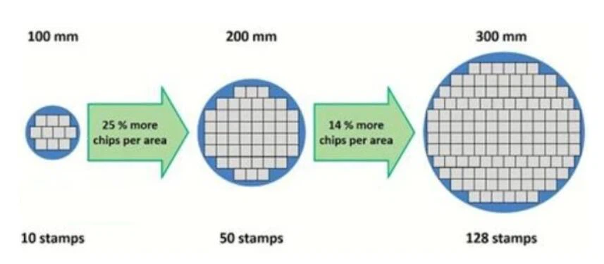
That is, compared with traditional LED displays, MicroLED is different in every aspect of die, packaging, integration process, backplane, driver, etc.-Therefore, we can see that the hot LED large-screen manufacturers of MicroLED concept products in 2021 have expressed their views.
Wafer Bonding method
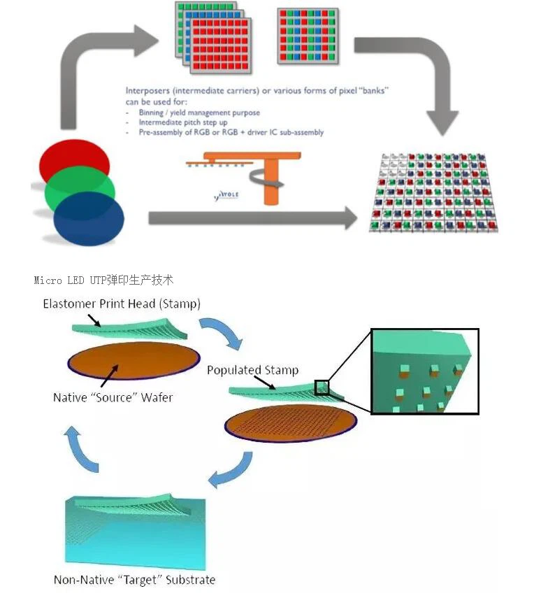
Process flow in practical application of μTP technology
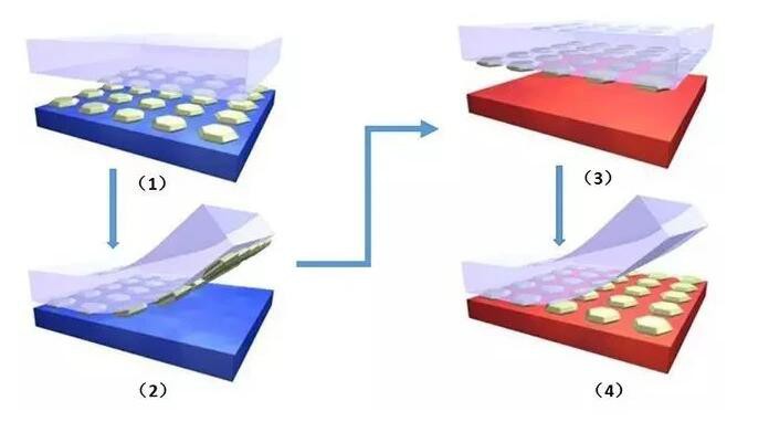
Surface mount technology has already achieved mass transfer technology production in MINI LED, but it needs actual combat verification in MicroLED production.
Although MicroLED displays are very expensive compared to traditional LCD and OLED panels, they have advantages in brightness and energy efficiency, making them an attractive alternative in ultra-small and ultra-large applications. Over time, the MicroLED manufacturing process will enable suppliers to reduce production costs. Once this process enters a mature period, MicroLED sales will begin to rise.
Let’s take an example to illustrate this trend. By 2026, the manufacturing cost of 1.5-inch microLED displays for smart watches is expected to drop to one-tenth of the current cost. At the same time, the manufacturing cost of the 75-inch TV display will be reduced to one-fifth of the current cost within the same period of time.
The manufacturing level is expected to reach the maturity threshold in 2024. Although acceptance has increased, microLED shipments in 2026 will still only account for 0.4% of the global flat panel display market. However, since this year’s shipments are close to 16 million, it will enter the mass market and lay the foundation for wider applications in the next few years.
In the past two years, the Mini LED industry will rapidly replace traditional display technology. In 2021, the electronic display industry such as vehicle display, home appliance display, conference display, and security display will launch a general attack to continue until Micro LED mass production technology stabilizes.


